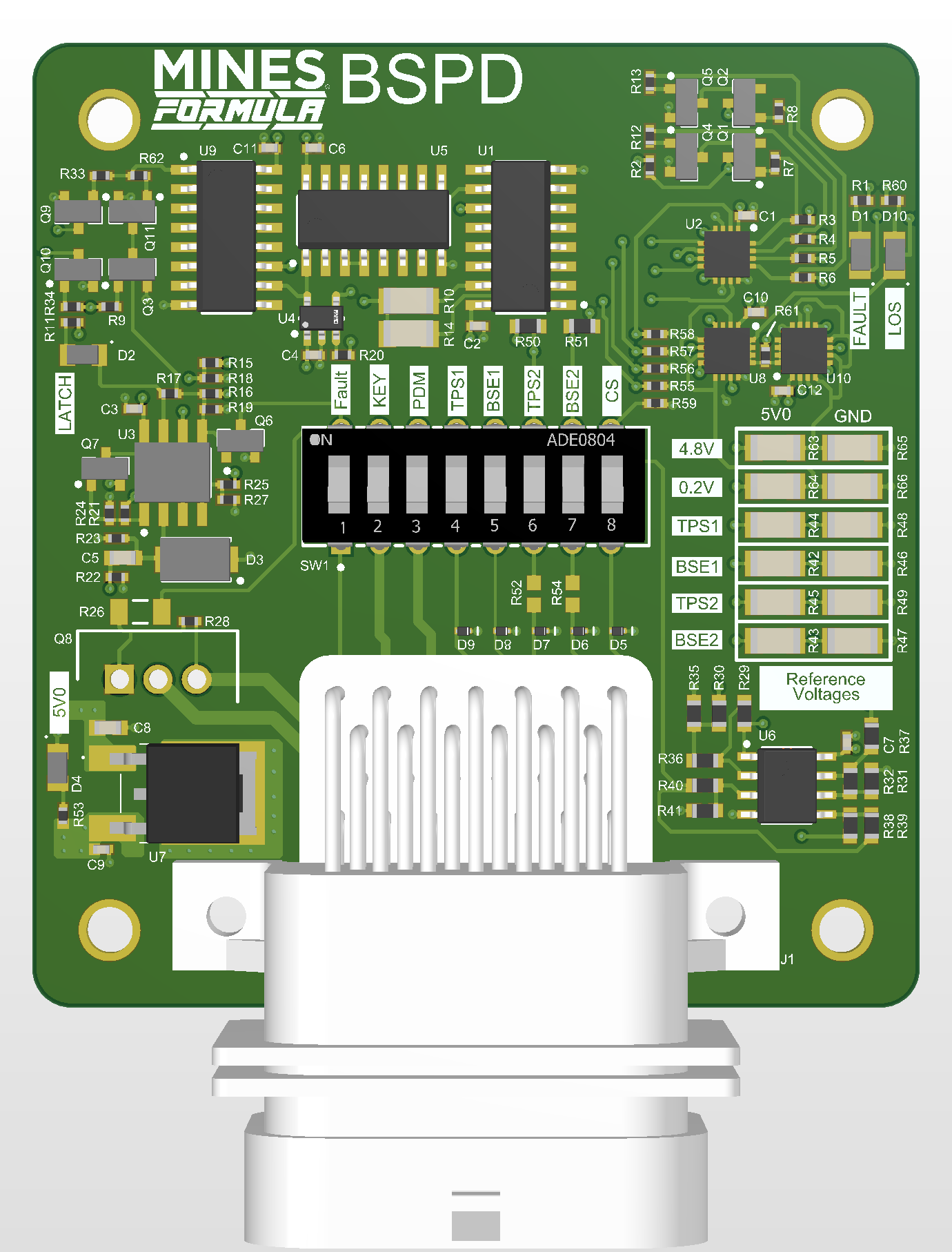
Formula SAE Brake System Plausibility Device (BSPD v3.0)
A custom, hardware-defined safety interlock engineered to comply with strict Formula SAE vehicle safety mandates. The circuit continuously monitors critical powertrain and braking dynamics, asserting an immediate and irreversible shutdown when simultaneous hard braking and high throttle/power demand is detected, or upon a sensor Loss of Signal (LOS) fault.
1. Executive Summary & Design Objectives
To comply with the Formula SAE non-programmable safety mandate, the BSPD v3.0 is implemented entirely using discrete analog and digital logic components—eliminating microcontrollers, FPGAs, and configurable CPLDs.
Conventional student designs typically rely on analog RC integration for fault timing, leaving them vulnerable to dielectric aging, engine-bay thermal drift, and nuisance trips caused by the rapid braking "pump-up" effect. BSPD v3.0 completely replaces analog timing circuits with a deterministic, clock-driven digital counter architecture, active dynamic range expansion stages, an asymmetric fast-discharge startup interlock, and a hardware-latched high-side shutdown driver.
2. Technical Specifications & Rule Compliance
| Parameter | Specification / Value | Design Context & Standard |
|---|---|---|
| Plausibility Delay (IC) | 1.00 s ± 1.5% | FSAE IC.4.8.4 (BSE Active + TPS > 10%) |
| Plausibility Delay (EV) | 0.50 s ± 1.5% | FSAE EV.8.7.2 (BSE Active + Power > 5 kW) |
| Loss of Signal (LOS) Delay | 100 ms ± 1.5% | FSAE IC.4.8.5 (Sensor Out-of-Range <0.5V or >4.5V) |
| Logic Architecture | 100% Non-Programmable Discrete | Zero firmware / microcontrollers (FSAE Compliant) |
| Reset Behavior | Power cycle Primary Master Switch | FSAE IC.4.8.6 (No dashboard/cockpit reset allowed) |
| Supply Voltage | +12V Nominal (LV Bus), +5.0V Regulated Logic | Automotive transient protection & reverse polarity clamp |
| Sensor Channels | 4-Channel Analog (0.50V – 4.50V) | BSE Primary, TPS Primary, BSE Comp, TPS Comp |
| Telemetry Interface | Dual Open-Drain Reporting Lines | Isolated Active-Low reporting to vehicle PDM / Datalogger |
3. Architectural Overview & Signal Flow
The board architecture divides signal processing into distinct stages: sensor conditioning, window comparators, differential expansion, dual synchronous timing engines, power-on blanking, and the safety shutdown latch.
4. Engineering Design Decisions & Trade Studies
4.1 Timing Engine: Deterministic Digital Counter vs. Analog RC Integrator
Conventional student designs often employ analog RC charging circuits with threshold comparators. BSPD v3.0 eliminates this failure mode by replacing analog RC integration with a digital binary counter driven by a precision silicon clock reference.
Conventional Analog RC Timing
- Timing Accuracy: Poor (±15% to ±25% across capacitor dielectric tolerances).
- Thermal Drift: High susceptibility to engine-bay thermal swings and dielectric aging.
- Reset Dynamics (Pump-Up): Slow exponential decay (5τ). Rapid intermittent pedal taps cause charge accumulation and premature false trips.
- Verification: Difficult to guarantee exact compliance windows during tech inspection.
BSPD v3.0 Digital Counter Engine
- Timing Accuracy: Precision (±1.5%), governed strictly by silicon oscillator stability.
- Thermal Drift: Frequency-locked silicon timebase across -40°C to +125°C.
- Instantaneous Clear: Asynchronous clear resets counter to zero in nanoseconds when fault drops (zero pump-up memory).
- Deterministic Verification: Guaranteed cycle count:
t_trip = (2^(n-1)) / f_clk.
4.2 Clock Generation & Distribution Network
Generating synchronous timebases for both the 100 ms LOS channel and the 500 ms / 1.0 s Plausibility channels required evaluating multiple clock topologies:
| Approach | BOM & Assembly Cost | Footprint | Thermal & Frequency Stability | Tradeoff Decision |
|---|---|---|---|---|
| 555 Timer RC Network | Low IC cost; expensive precision C0G caps | Large | Poor (>5% drift over temperature) | Rejected due to temperature jitter |
| Dual Silicon Oscillators (LTC6900 x 2) | High (>$12.00 incremental BOM) | Compact | Excellent (<0.09% / °C) | Rejected due to unnecessary BOM cost |
| Single LTC6900 + Logic Divider | Optimal BOM Balance | Compact (SOIC-8) | Excellent (Sub-1% accuracy) | Selected Architecture |
4.3 Logic Synthesis: Open-Drain Bus vs. Dedicated Logic ICs
To aggregate multi-channel faults while optimizing Design for Manufacturing (DFM) on prototype SMT lines:
- Open-Drain Bus Aggregation: Comparators utilize open-drain output stages tied to a shared pull-up bus. This allows wired-OR fault detection across multiple sensor channels without risk of output stage contention or supply-to-ground shoot-through.
- Discrete Dual Series N-Channel MOSFET AND: Rather than adding dedicated 74-series logic gate ICs—which incur unique part tooling surcharges—series low-side N-channel MOSFETs synthesize the plausibility interlock.
5. Detailed Circuit Block Implementation
5.1 Multi-Stage Sensor Interface & Loss of Signal (LOS) Detection
The analog front-end processes four sensor channels: Primary and Complementary Brake System Encoder (BSE) and Throttle Position Sensor (TPS).
- Operating Range: 0.50 V to 4.50 V nominal.
- LOS Fault Detection: Pull-up and pull-down networks ensure that an open circuit, disconnected sensor connector, or short-to-rail immediately forces the line into out-of-bounds bands (<0.50V or >4.50V).
- Resistive Divider Calibration: Standardized 1206 SMD packages were deliberately selected for all divider ladders to allow rapid benchtop and trackside re-biasing during vehicle calibration without requiring board respins.
5.2 Active Dynamic Range Expansion (Differential-Summing Front-End)
In electric powertrain configurations, DC current sensor outputs exhibit a narrow differential output voltage (2.50 V zero-current reference to 2.60 V at the 5 kW fault threshold). To avoid false trips caused by electrical noise in a high-voltage inverter environment, a custom two-stage op-amp front-end amplifies the fault delta by 10× while preserving the nominal zero-current baseline for LOS monitoring.
Design Impact: Expands a narrow 100 mV fault margin into an easily detected 1.00 V swing above baseline, completely eliminating comparator sensitivity jitter without distorting the lower 0.0 V – 2.5 V range required for open-circuit LOS detection.
5.3 Startup Interlock with Asymmetric Fast-Discharge
To prevent spurious shutdown assertions while power rails and sensor analog outputs stabilize during vehicle boot-up, an analog startup interlock circuit forces a 1.39 s blanking window.
When the vehicle master switch is cycled off, Schottky diode D3 forward-biases, routing stored charge through a 10 kΩ resistor to reset the capacitor in under 500 ms (5τ), guaranteeing proper blanking protection even during rapid consecutive power cycles.
5.4 Safety Latch & Master Shutdown Loop Interfacing
- Hardware Latch: Built around a high-speed comparator with positive feedback. Once the active-low SHUTDOWN net is driven low, the latch transitions low and cuts off gate bias (V_GS = 0V) to the high-side shutdown pass-through switch.
- FSAE Rule IC.4.8.6 Compliance: The latch contains zero manual reset paths or buttons. Recovery requires cycling the vehicle Primary Master Switch to remove logic power.
- High-Side SDC Switch: P-channel MOSFET placed in series with the vehicle's Brake Over-Travel Switch (BOTS) loop.
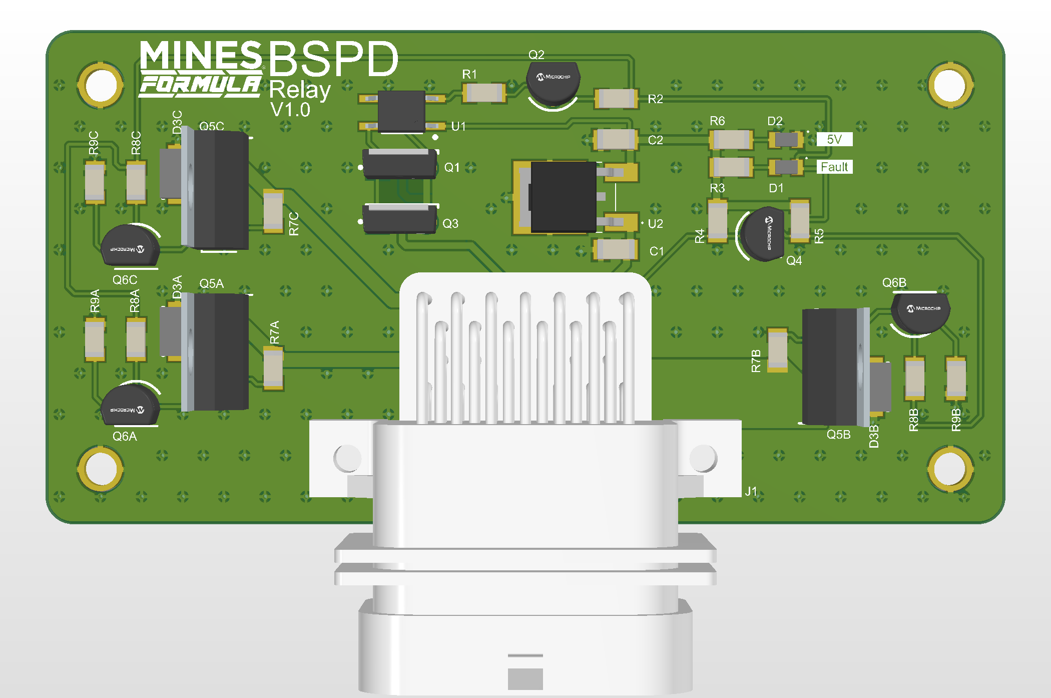
- Isolated Telemetry: Independent open-drain N-channel MOSFETs report fault status to the vehicle Power Distribution Module (PDM) with complete electrical isolation.
6. Key Achievements & Engineering Impact
- Deterministic Reliability: Replaced non-deterministic analog RC timers with synchronous digital counters, eliminating nuisance trips caused by thermal drift and rapid braking cycles.
- 100% Rule Compliance: Fully verified against Formula SAE non-programmable mandates with integrated dynamic range expansion for EV current sensing.
- Optimized DFM & SMT Assembly: Standardized 1206 resistor tuning networks, open-drain bus aggregation, and discrete SOT-23 MOSFET logic to minimize prototype tooling costs.